


Hopper: Nvidia presents new H100 GPU
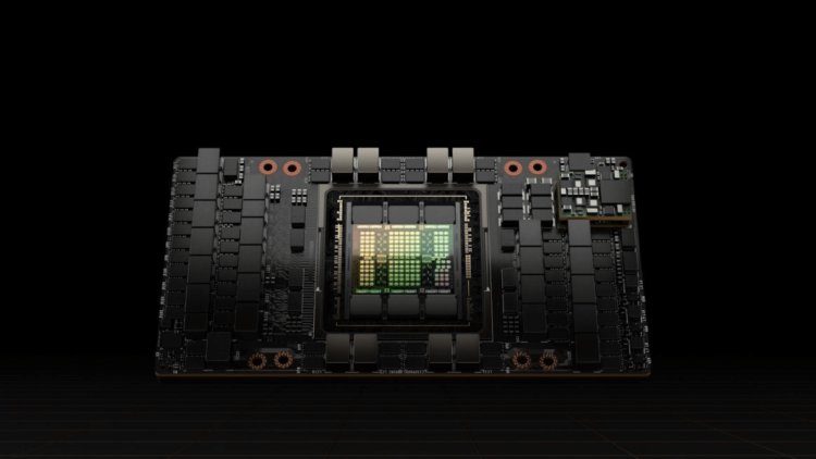
Jensen Huang demonstrated the new hopper architecture alongside the first GPU, the H100, during the GTC 2022 keynote. The hopper design is reported to be substantially more powerful than its predecessor Ampere, with over 80 billion transistors and a TDP of 700 W, among other things.
The keynote lecture at this year's GTC focused on Nvidia's AI solutions' multiple application areas, such as autonomous driving and weather forecasting, as well as the all-encompassing "omniverse." The debut of the hopper architecture alongside the first GPU, the H100, was undoubtedly the most fascinating thing for GPU fans.
The Hopper architecture is intended to provide a considerable performance boost over its predecessor, the Ampere, and to power the next generation of AI data centers. Nvidia describes the H100 GPU as the world's largest and most powerful accelerator. "The Nvidia H100 is the engine of the global AI infrastructure that enterprises are adopting to propel their AI-driven operations," Nvidia CEO Jensen Huang stated.
The H100 is made on TSMC's 4-nanometer process and contains 80 billion transistors. Furthermore, the H100 is believed to be the first GPU to support PCI-Express 5.0 and the first to employ HBM3, allowing for a 3 TB/s memory bandwidth. Twenty of these H100 GPUs should be able to handle all of the world's Internet traffic.
A new Transformer engine, numerous 2nd generation instances driven by MIG technology, Confidential Computing, and 4th generation Nvidia NVLink and DPX commands are among the other H100 features. Nvidia's website describing the hopper architecture has more information on the features stated. The H100 GPUs should have a wide range of applications as well. As a result, they may be utilized in any form of a data center, and eight of them are merged in a DGX H100, Nvidia's 4th generation DGX system.
These devices are touted to provide 32 petaflops of AI performance with new F8 precision. Each GPU in a DGX-H100 system is likewise linked through NVLink and has a transfer rate of 900 GB/s, which is roughly 1.5 times that of the preceding Ampere architecture. An additional NVLink switch can also connect up to 32 DGX-H100 nodes in a SuperPOD supercomputer. On the next page, you can find out which form factors the H100 will be available in and what the characteristics will be.
H100 in SXM form factor:
- eight GPCs, 66 TPCs, two SMs per TPC, 132 SMs per GPU
- 128 FP32 CUDA cores per SM, 16,896 FP32 CUDA cores per GPU
- four Gen 4 Tensor cores per SM, 528 per GPU
- 80 GiByte HBM3, 5 HBM3 stacks, ten 512-bit memory controllers
- 50 MiByte L2 cache
- 700W TDP
- 4th generation NVLink and PCI Express 5.0
H100 in PCI Express form factor:
- seven or eight GPCs, 57 TPCs, two SMs per TPC, 114 SMs per GPU
- 128 FP32 CUDA cores per SM, 14,592 FP32 CUDA cores per GPU
- four Gen 4 Tensor cores per SM, 456 per GPU
- 80 GiByte HBM2e, 5 HBM2e stacks, ten 512-bit memory controllers
- 50 MiByte L2 cache
- 4th generation NVLink and PCI Express 5.0