


IBM shows new nanosheet transistors
IBM has announced a new 2nm manufacturing process that uses four nanosheets per transistor. This should result in good switching properties while consuming little space.
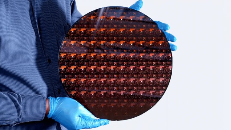
IBM's research group has revealed a new semiconductor manufacturing technique: the business successfully produced a 300 mm wafer utilizing the new 2 nm production technology. Although this has no influence on clients right now due to a lack of market maturity, this and comparable practices are likely to become common in a few years.
IBM claims that it will use the second generation of nanosheet transistors to achieve the 2 nm node. The gate encloses four conduction channels, resulting in a very wide contact area between the conduction channel and the gate while taking up no additional space. In turn, this contact surface ensures good conduction qualities.

In comparison, major foundries continue to use FinFET transistors, in which a single conduction channel protrudes vertically from the wafer and is thus in touch with the gate on three surfaces.
Gate-All-Around (GAA) or nanowire transistors, which entirely encircle tiny conduction channels, are predicted to succeed in this technology. In turn, nanosheets expand on this method by becoming wider and therefore reaching an even bigger contact area.
IBM predicts a 45 percent performance boost over current 7 nm processes, or a 75 percent reduction in energy consumption, with the new 2 nm production.
When compared to TSMC's 5 nm technology, which is slated to be deployed on a big scale by the end of the year, the benefits may not be as significant, but they should still be significant. In the future, it appears that semiconductor production will make even greater strides.